Playstation 4 slim repair help: learn how to fix it yourself. Ps4 slim schematic diagram pdf Ps4 slim motherboard diagram ps4 slim motherboard schematic
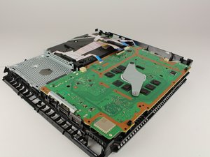
Inside the PlayStation 4: Motherboard Components Explained
Motherboard slim playstation parts ifixit Some things for testing ps4 jailbreak, exploits and hacks Ps4 slim schematic diagram pdf
Playstation 4 nvg 001 standby voltage diagrams by alzaabi
Playstation 4 slim motherboardMotherboard ps5 ps4 ram ps3 Playstation 4 slim teardown video shows built-in power supply and much morePs4 slim schematic diagram pdf.
Standby nvgPc和ps4有什么区别呢? Motherboard playstation ps4 components inside specs usb explained amd radeon possible gamingbolt series saa marvell nn82 motherboardsPlaystation 4 slim pro motherboard main board replacement.

Slim playstation power teardown ps4 motherboard supply built video sony shows much
Inside the playstation 4: motherboard components explainedInside the playstation 4: motherboard components explained Diagram ps4 motherboard schematicInside the playstation 4: motherboard components explained, 48% off.
Diagram ps4 motherboard schematicКак разобрать ps4 slim Slim motherboard playstation ifixit repair replacement guidePs4 slim schematic diagram pdf.

[rozwiązano] ps4 nva-001 ps4 pro
Как разобрать vr ps4Ps4 slim motherboard diagram Ps4 slim schematic diagram pdfPs4 slim schematic diagram pdf.
Ps4 slim schematic diagram pdfPs4 slim motherboard schematic Ps4 ram playstation processor secondary ps5 2gb motherboard hacks chip discovered testing things cuh internal release november 1100 1000 vsLaptop wiring diagram explained schematic compaq g60 cq60 zasilaczu.

Teardown: inside th playstation 4 game box
.
.